Crystal Orientation in CVD Diamond Plates - (100) vs (110) vs (111)
%20vs%20(110)%20vs%20(111).jpg)
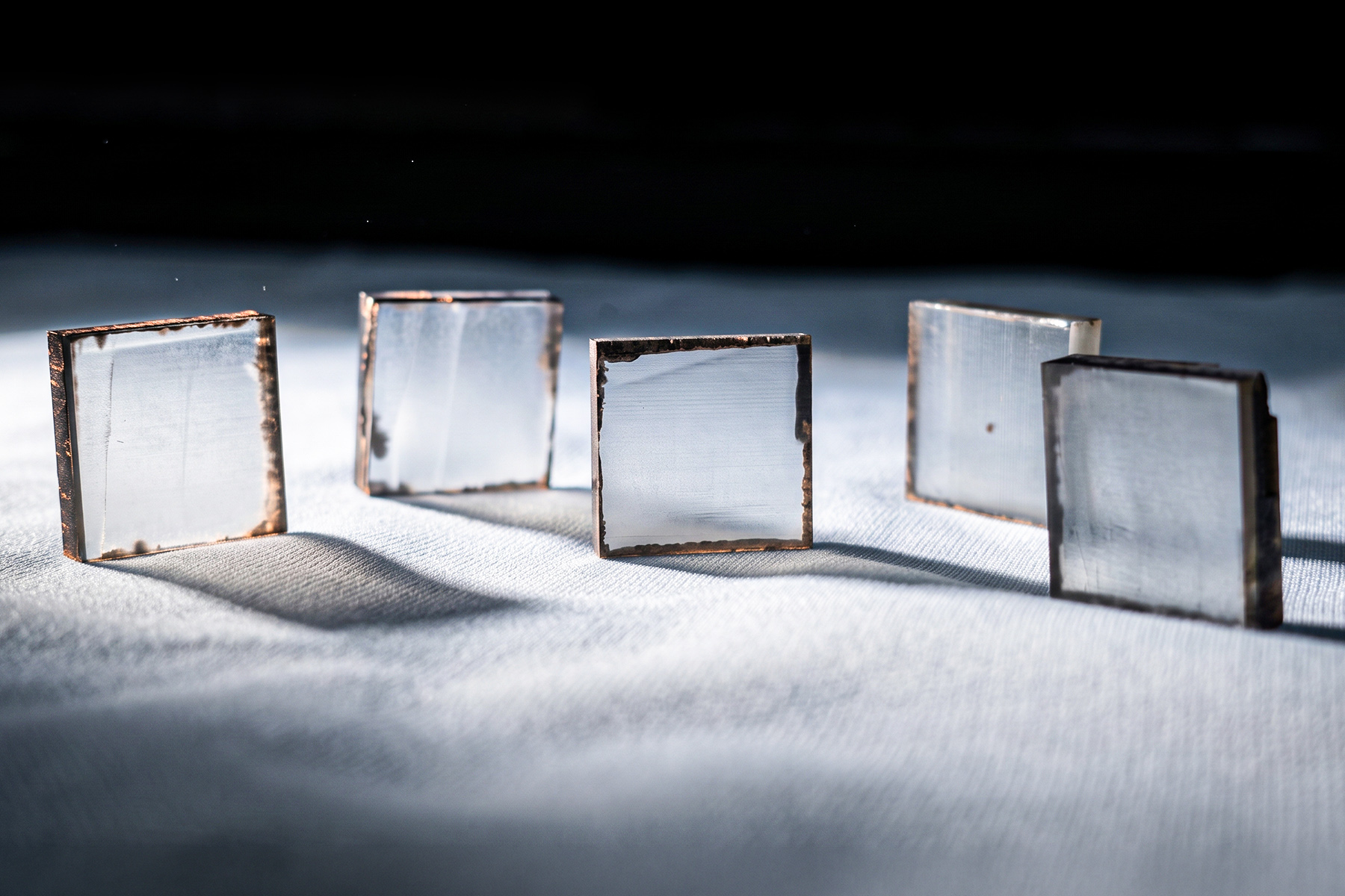
The physical, mechanical, optical and electrical properties of a CVD diamond plate are dependent on its crystallographic orientation. The orientation of the primary exposed area of a CVD diamond plate governs more than the hardness. It determines how the diamond grows, how the impurities and defects are distributed and its performance in electronic, optical, and thermal applications. In CVD, this begins at the seed. Diamond is deposited atom by atom onto a seed crystal, and the seed's orientation sets the orientation of everything grown on it and which is why (100) appears on most CVD specifications.
Hence, it is important to understand the three main crystal orientations - (100), (110) and (111) when selecting the right diamond plate for specific applications.
Crystal Orientation in CVD Diamonds
Crystal orientation is how the carbon atoms are arranged inside the diamond crystal. This arrangement defines the direction of the crystal planes identified as (100), (110) and (111). Using Miller's numbering system, scientists identify different crystal orientations. An ordered triplet of integers (hkl) is used to determine the plane.
Each value in the triplet represents the reciprocal of the plane's intercepts along the three primary crystallographic axes of the unit cell. When it comes to the diamond industry, the (100), (110) and (111) planes are designated as 4-point, 2-point and 3-point planes.
A CVD-grown rough diamond has six faces, and the orientation of these faces depends on the crystal growth and the planes that develop during the process. The required crystal plane is not created afterward; rather, the diamond is cut and polished to make the desired plane available at the surface.
The choice of which plane to expose depends largely on the end application.
Main Crystal Orientations
Crystal orientation determines the direction in which the atoms of the diamonds are arranged. Understanding the crystal orientation is important for cutting tools and semiconductor applications. Diamonds possess a face centered cubic crystal system also known as diamond cubic lattice systems and feature three main crystal orientations.
100 Crystal Orientation (Cube Face)

The 100 crystal orientation has a cube face where atoms are arranged evenly and is easy to machine stably.
Characteristics
a. Stable surface structure
The (100) crystal orientation is the most commonly used surface for the growth of high-quality single-crystal CVD diamonds. In this CVD process, the hydrogen atoms attach to the diamond surface during CVD growth and rearrange the surface atoms into a more stable structure. This results in a more stable surface allowing new carbon atoms to be arranged in an organized way.
b. Step-Flow Growth
Diamond grown on a (100) seed plate mainly happens through a process called step-flow growth. In this process, the carbon atoms (mainly from methyl radicals, CH3) attach to the edges of tiny atomic steps and gradually move them forward. This growth method works best across a wide range of temperatures, methane concentrations and chamber pressures.
Key Properties
The following are the key properties of 100 crystal orientation:
1. Faster diamond growth
The (100) crystal orientation has a well-optimized growth process. This allows the growth process to become faster than many other orientations. It also allows manufacturing of thicker diamond plates and larger substrates in less time.
2. Suitable for large diamond plates
The stable growth process of (100) crystal orientation is commonly used to manufacture millimeter-thick and large single-crystal CVD diamond plates.
3. Resistance to laser damage
Their ability to handle higher laser energy without surface damage makes them ideal for laser processing and precision micromachining.
4. Easy to polish
The 100 crystal orientation allows the material to be removed efficiently along the four specific directions. This accelerates the entire polishing process.
Application Areas
1. Power Electronics
The (100) crystal orientation is widely used in high-power semiconductor devices since it has low defect density and stable crystal growth. These properties support the fabrication of high-voltage and high performance components. Schottky Barrier Diodes, Field-Effect Transistors and High-Power Microwave Switches are few examples of such applications.
2. Advanced Thermal Management
The exceptional thermal performance allows the heat to spread evenly and prevents overheating. This in turn helps improve the reliability of high-power electronic systems. Some common examples of these applications include: high-density RF power amplifiers, diode laser arrays and micro-processor hotspots.
3. RF Applications
The (100) crystal orientation provides excellent optical transparency across a broad wavelength range. This makes it suitable for high-power optical and microwave systems. Some examples of this includes: high-power CO₂ laser output windows, gyrotrons, synchrotron beamline windows, and terahertz and far-infrared optical components.
111 Crystal Orientation
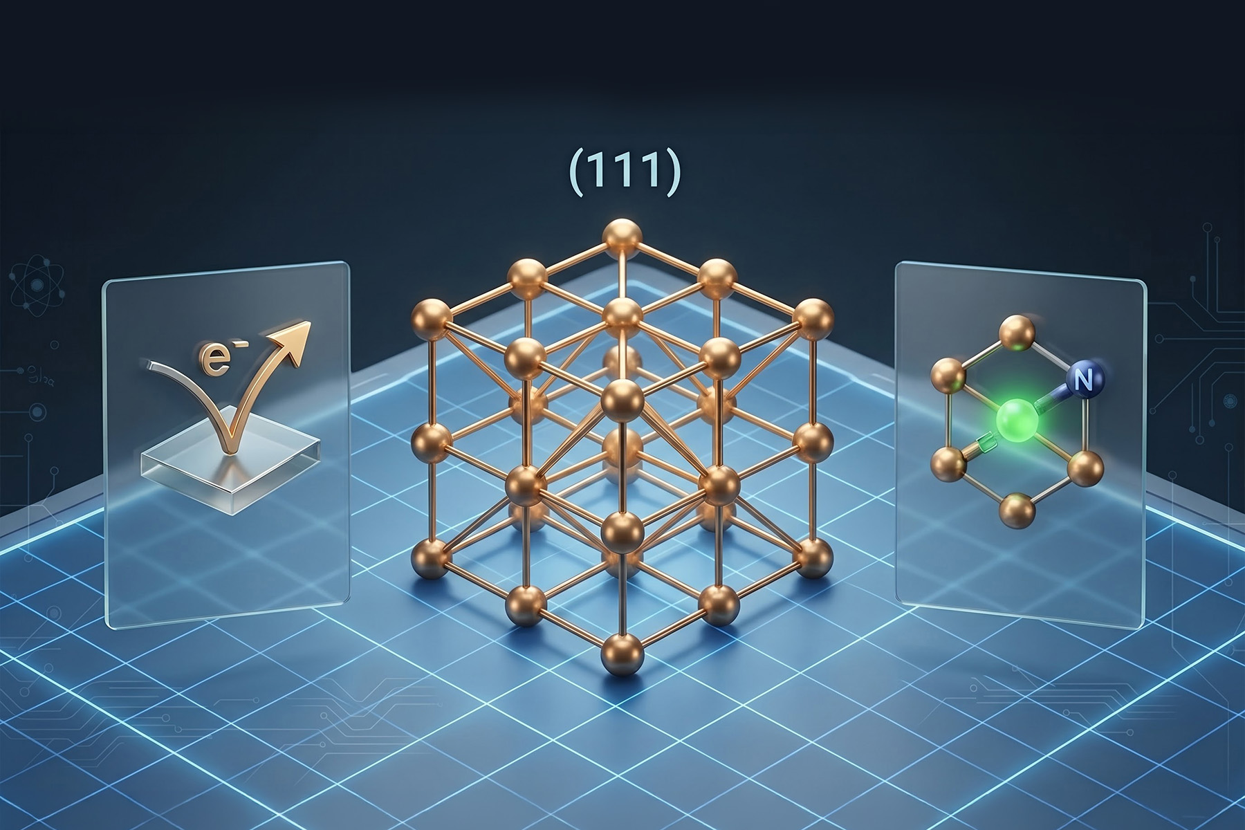
The (111) crystal orientation features a tightly packed surface in diamond. In this case, the carbon atoms are positioned closer together than in any other crystal orientation. This results in distinctive surface characteristics.
Characteristics
1. Negative electron affinity (NEA): The (111) crystal orientation has negative electron affinity (NEA). This facilitates electron emission from the surface with ease. This makes it particularly valuable for sophisticated electronic and quantum applications.
2. Crystal Defects: The risk of developing crystal defects is higher in (111) crystal orientation. Some of the common defects are penetration twins, stacking faults and unwanted sp² carbon inclusions during CVD growth.
3. Specific Growth Conditions: The process of growing (111) crystal orientation must be done by taking into account precise growth conditions. This is to ensure that there are minimum defects and the crystal quality is maintained.
Key Properties
1. Ideal for NV Centers: The (111) crystal orientation is valuable for creation of "Nitrogen-Vacancy (NV) centers". NV centers are atomic-scale defects ideally used in different quantum technologies including quantum sensing, communication and computing.
2. Superior Light Collection: The precise alignment of NV centers in (111) diamond plates results in light which is easier to collect. This offers the following advantages:
- Excellent light collection efficiency
- Clear optical signals
- Reliable performance in quantum sensing and imaging applications
3. Easy to integrate dopants: This crystal orientation is highly valuable for integrating dopants such as nitrogen and boron during the CVD growth process. Hence, (111) crystal diamond plates are a preferred choice for electronic and quantum devices.
4. Excellent Hardness: The (111) crystal orientation features the hardest surface orientation of diamond. Due to this exceptional hardness, it is resistant to wearing which makes them ideal for demanding industrial applications.
Application Areas
The following table represents the different application areas of (111) crystal orientation:
110 Crystal Orientation
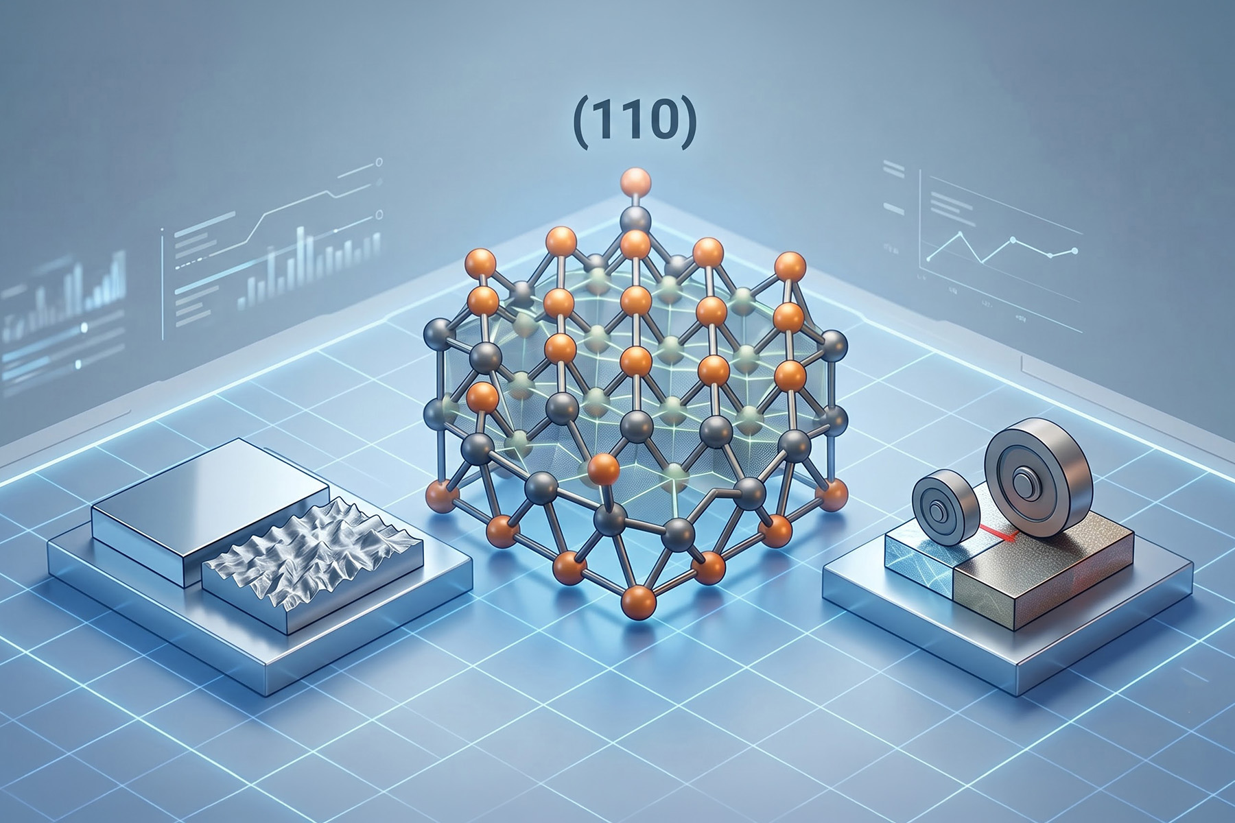
The 110 crystal orientation features a rectangle surface which is though not easy to machine but has a better wear resistance. This is especially useful for cutting tools and high-precision optical applications.
Characteristics
1. Atomic Structure
The (110) crystallographic orientation also known as the dodecahedral plane has an uneven and ridged surface right at the atomic level. The carbon atoms on this surface are arranged in a zig-zag pattern. Also, every surface atom has one dangling bond extending outward at an angle from the surface normal.
2. Growth Challenges
When it comes to growing diamond on a 110 substrate, maintaining a smooth and stable surface is difficult compared to other crystal orientations. Also the 110 crystal orientation is prone to chemical roughening making the surface highly susceptible to impurities.
3. Defect-Free Growth
For defect-free growth, it is important that manufacturers carefully control the gas mixture, ensure low nitrogen contamination and create excellent plasma conditions throughout the growth process.
Key Properties
1. Physical Properties: The (110) crystal orientation features the same core physical properties as bulk diamond including the speed of sound, Young's modulus and a dielectric constant of 5.71. Additionally, their surface-specific properties are different from (100) crystal orientation.
2. Resistance to Laser Damage: When subject to laser energy, the 110 crystal orientation gets damaged at lower energy levels compared to 100 crystal orientation. This makes 110 crystal orientation more prone to laser-induced changes and hence orientation is an important consideration in any laser-based processing.
3. Polishing Behaviour: The 110 crystal orientation surface has preferred directions that allow for quick material removal and smooth flattening. However, there is one shortcoming here that even a slight deviation from these directions will result in wear resistance to rise sharply. This sensitivity highlights the varying hardness of the diamond across the crystal.
Key Takeaways
The key takeaway is that the direction of the plane plays an important role in the growth of CVD diamond. The same material cut along different planes will differ in how it grows and how it performs as a finished component. Choosing the right orientation will ultimately determine how the final diamond plate will perform.
Since lab-grown diamonds are becoming more valuable in electronics, optics and quantum technology, selecting the right crystal orientation will help get the most from this remarkable material.
Frequently Asked Questions
Here are some interesting FAQs on Crystal Orientation in CVD Diamond Plates:
“redefining one diamond layer at a time”
More Articles
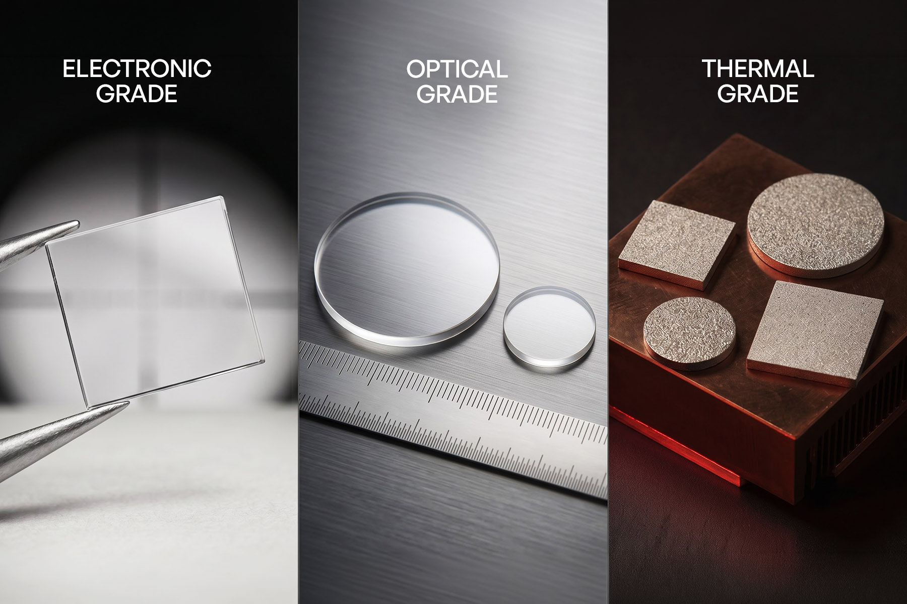



Aga9 Systems is a lab-grown diamond manufacturing company dedicated to harnessing the valuable properties of CVD diamonds for industrial applications. We at Aga9 Systems manufacture more than lab-grown diamond plates, we are dedicated to creating brilliance ethically, sustainably and with maximum resource efficiency.