How Lab-Grown Diamonds Are Shaping The Future of Electronics?
Lab-grown diamonds today are standing at the forefront for revolutizing demanding industries like electronics. Today manufacturers of electronic devices have started realizing the importance of lab-grown diamond plates to improve performance and efficiency. Lab-grown diamonds have strikingly better properties compared to other semiconductors such as silicon (Si) and silicon carbide (SiC). They have a higher electrical breakdown, thermal conductivity and excellent carrier mobility.
In this blog, we will explore how diamonds are improving the performance of electronic devices and what it means for the industry’s future.
Importance of Diamonds in Electronics
Diamonds are often regarded as an ultra-wide bandgap semiconductor offering exceptional properties that are far better than many known materials. In addition to its known hardness (Mohs scale 10), diamond showcases the highest thermal conductivity at room temperature. It also features exceptional chemical inertness and optical transparency.
These properties position diamonds as a great substrate material for devices to operate in extreme environments. Industrial applications where the tendency of occurrence of voltage, heat and intense radiation is high, will benefit immensely with the use of lab-grown diamonds. The strategic importance of LGDs, therefore, lies in their ability to unlock previously unattainable performance. These are critical for aerospace, defense, and high-speed computation including high-efficiency electric vehicle power systems.
Benefits of Lab-Grown Diamonds for Electronics

Lab-grown diamonds are a sustainable alternative to other semiconductor materials since they combine the benefits of thermal, mechanical and optical properties. This striking combination of properties outperforms materials such as SiC and Si.
1. Ultra-Wide Bandgap Semi-Conductor
Si (1.10 eV) and SiC (3.26 eV) possess a smaller bandgap than that of diamond (5.47 eV) which falls under the category of Ultra-Wide-BandGap (UWBG) (>4 eV). Larger bandgap implies the requirement of the large amount of the energy to move an electron from the valence band to conduction band. In other words, UWBG can sustain higher operational voltage owing to higher electrical breakdown (~ 10 MV/cm). Therefore, the diamond based devices can easily perform operations at high voltages, high current, and high temperatures.
2. Smaller Device Dimensions
Being a UWBG, synthetic diamonds can offer smaller device fabrication as compared to Si and SiC based devices. Diamond based devices will require thinner films and therefore, the electrical path resistance will also be lower. Thus, due to the thinner film fabrication, the final device dimensions can become compact.
3. High Frequency Operation
Synthetic single crystal diamond offers higher electron and hole mobility which can result in faster switching of the charge carriers. Therefore, a reduced switching losses in diamond based devices will be observed which ultimately will result in more efficient devices.
4. Optoelectronic Device Fabrication
Synthetic diamond can also find its application in fabrication optoelectronic devices such as deep ultraviolet (UV) detectors and sensors. A material can be exploited as a UV detector if it is able to transmit the UV rays through it. Diamond has significantly larger transparency than that of existing wide bandgap materials (~ SiC). Diamond based UV detectors can easily find their application in the field of UV-LED fabrication, space applications, and high energy physics applications.
5. Excellent Switching Speed
Lab-grown diamonds also feature superior voltage and thermal management which significantly facilitates smooth and fast device operation. The electrons present in diamond semiconductors are responsible for high switching speeds, excellent stability and rapid heat dissipation. Hence, electronic devices with lab-grown diamond plates as a material will be able to handle heat much better than next-generation electronics.
Practical Applications of Lab-Grown Diamonds in Electronics
In addition to being the hardest material, lab-grown diamonds possess superior thermal conductivity which makes them a good fit for high-performance electronics. The outstanding performance of lab-grown diamonds can be seen in the following key applications:

1. Switches and Diodes
The high breakdown electric field and mobility of lab-grown diamonds makes them perfect for high-power switching applications. This enables them to handle high voltages and current without causing any degradation. Diamond based power switches and diodes are beneficial in the following applications:
- High-power converters and inverters in electric vehicles
- Solid-state circuit breakers
2. Heat Spreaders
Overtime too much heat build up will result in degradation and hamper device performance. Lab-grown diamonds are an excellent material to manage heat effectively and that too far better than that of conventional materials like copper and silicon. Lab-grown diamond heat sinks have the ability to absorb and dissipate heat away from sensitive components. This ensures a stable and reliable performance even during the toughest industrial applications.
3. Diamonds as Semiconductors
Over the years, the industry has relied on silicon for electronic devices. But with lab-grown diamonds the benefits are seen increasing manifold. Diamonds are being integrated into semiconductors primarily due to their outstanding ability to withstand extreme temperatures and voltages. From industries like aerospace to automotive engineering, diamonds are seen making their invaluable mark.
Let us understand this with an example. Diamonds are being used in transistors to regulate signal in high-power devices. The superior thermal management property of diamonds reduces the risk of overheating which enhances the performance devices such as power grids and radio transmitters.
4. Quantum Computing
Another exciting opportunity for lab-grown diamonds lies in quantum computing. Diamonds contain nitrogen-vacancy (NV) centers which are small imperfections in the crystal. These imperfections act as stable quantum bits also known as qubits. The presence of qubits helps the development of quantum computers. These quantum computers work faster than traditional machines and will prove beneficial in areas such as cryptography and artificial intelligence.
Scattering heat is another factor seen in high-performance computing. Due to the high thermal conductivity of diamonds, they can ensure cooler operations which is a feature already being explored for servers, processors and lasers.
5. Smartphones
Diamonds have also made their way to smartphone technology. Screens made using diamonds are more likely to be scratch resistant and long-lasting. As we move ahead, we are integrating into smaller and more powerful processors. Here is where the use of diamonds can improve the computing speeds and lead to energy efficiency.
Conclusion
Lab-grown diamonds are changing the world of electronics. Engineers today are obsessed with the toughest form of carbon - diamonds. These diamonds can play an important role in developing power electronic devices, transforming sensing and communication technologies.
With unmatched thermal conductivity, breakdown voltage and superb mechanical strength they are proving to be far better compared to Si and SiC. Industries today are in constant need for faster, smaller and more energy efficient devices. This constant need is driving the demand for diamond-based components.
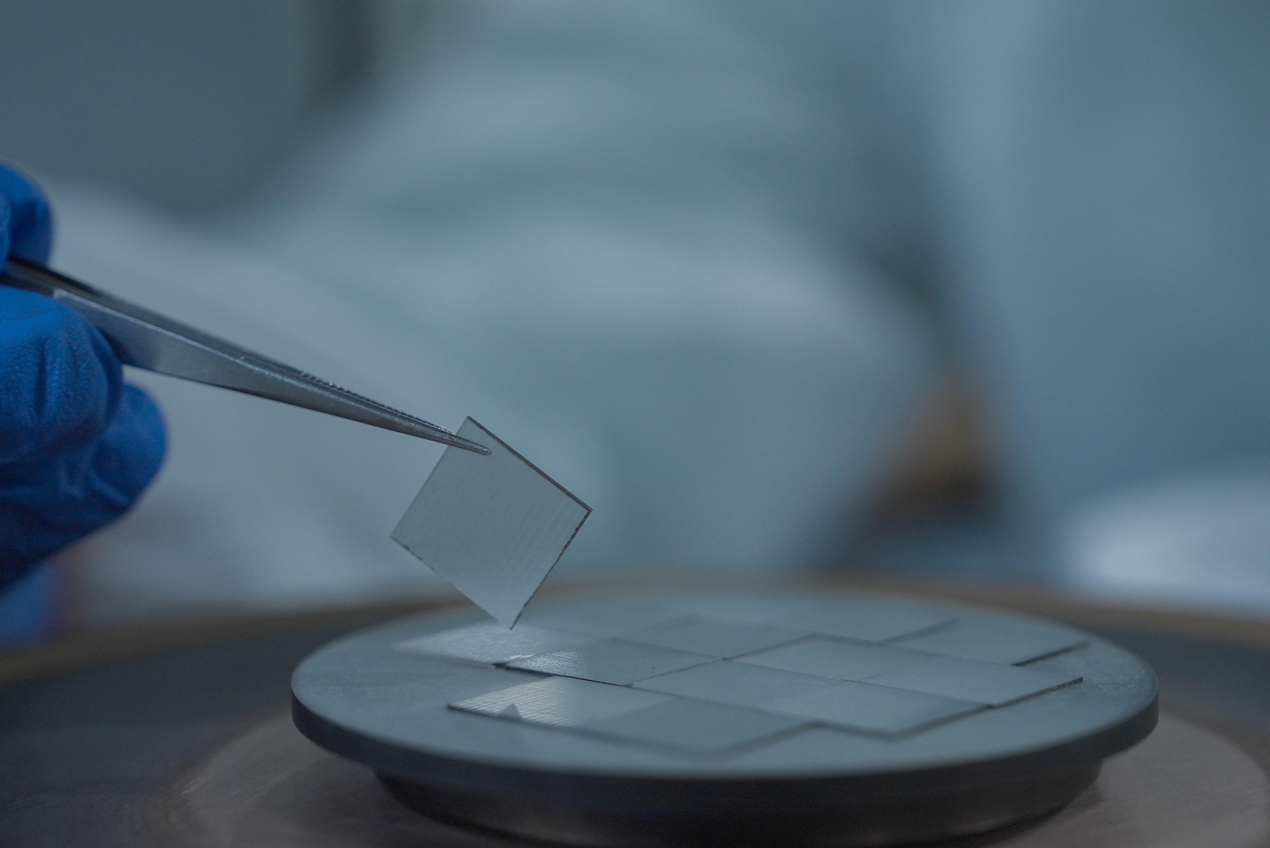
At Aga9, we are working at the forefront of that transformation. We are aimed at developing high-quality lab-grown diamond plates which are efficient, sustainable and technologically advanced. We offer both single crystal and polycrystalline diamond plates in customizable sizes and thicknesses to address demanding business requirements.
Frequently Asked Question
“redefining one diamond layer at a time”
More Articles


Aga9 is a lab-grown diamond manufacturing company dedicated to harnessing the valuable properties of CVD diamonds for industrial applications. We at Aga9 manufacture more than lab-grown diamond plates, we are dedicated to creating brilliance ethically, sustainably and with maximum resource efficiency.